
From Zero to FPGA Engineer: Why We Must Master Chip Design
Bismillahir Rahmanir Rahim
FPGA Engineering Blog Series: Welcome
Hello, my name is Ramiz Qurbanli. Welcome to my new blog series on FPGA Engineering. This series is designed to take you from the absolute basics of digital logic to designing custom chips using the hardware description language, Verilog.
Our Mission: Sovereignty Through Science
The purpose of this blog is to direct Muslim youth toward the sciences—specifically the field of chip design. Mastering this field will not only make you a high-demand talent in the global market but is also essential for the independence of our nations.
As you may know, a few major companies (mostly based in the US) dominate chip design and manufacturing. Recently, we have seen how geopolitical shifts and trade restrictions can limit a nation’s access to critical technology. I believe we must cultivate our own engineers so that we can eventually design and create our own hardware. That is why I have created this blog: to provide a path from Zero to FPGA Engineer.

Why FPGA?
You might ask, "Is FPGA the same as full chip design?" Technically, no—but it is the essential entry point. To become an FPGA engineer, you must master the core pillars of chip design: Digital Logic, Boolean Algebra, Transistor Physics, Combinational and Sequential Logic, Computer Architecture, and Memory Systems.
Chip design is a massive, multi-disciplinary field. While I won’t be teaching you how to manufacture nanometer-level transistors in a "fab" (fabrication plant), I will focus on the Logic Design and HDL (Hardware Description Language) phase. Companies like Nvidia, Intel, and AMD are often "fabless," meaning they design the logic and document it, then send those designs to specialized factories (like TSMC in Taiwan) to be printed.
HDL is the brain of the chip. By learning it, you gain the power to define exactly how hardware behaves.

What is an FPGA?
FPGA stands for Field Programmable Gate Array. In simple terms, it is a chip containing thousands of logic gates that are not "hard-wired." When we write HDL code and load it onto the FPGA, our code tells the chip which gates to connect and in what order.
Unlike a general-purpose CPU, an FPGA can be customized for a specific task, allowing for incredible speed and ultra-low latency.
Key Applications of FPGA Technology:
Defense & Aerospace: Radar beamforming, signal jamming, and radiation-hardened satellite processing.
Telecommunications: 5G/6G base station processing and high-speed network protocols.
AI & Data Centers: Hardware acceleration for Large Language Models (LLMs) and real-time encryption.
Finance: High-frequency trading (HFT) platforms where every nanosecond counts.
Medical: Real-time 3D reconstruction for MRI and CT scans.
Automotive: ADAS (Advanced Driver Assistance Systems) and LiDAR sensor fusion.

Our Learning Roadmap
We will not start with coding right away. To avoid being a "code monkey" who doesn't understand the underlying physics, we will build a foundation as true engineers.

Phase 1: The Digital Foundation
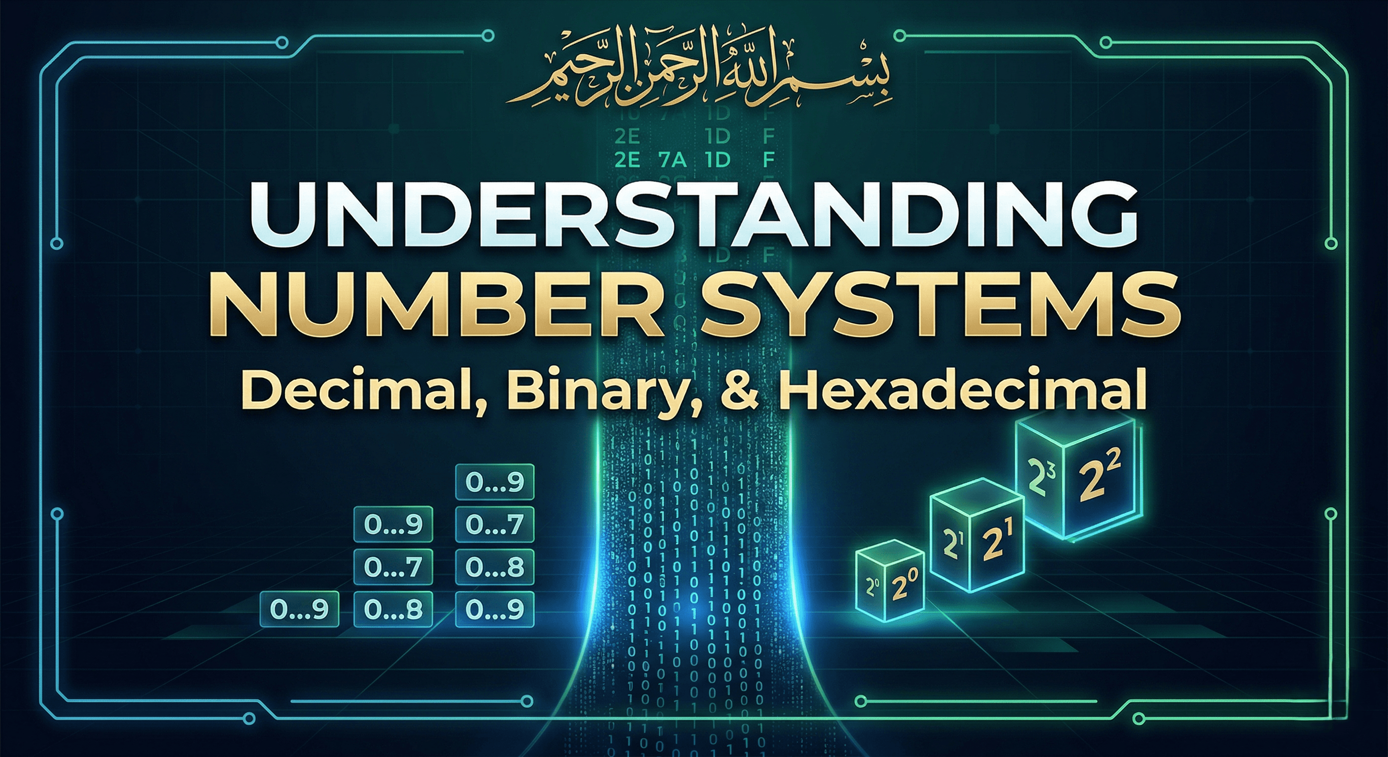
Logic Fundamentals: Number systems (Binary, Hex) and Two’s Complement.
Transistor Basics: How CMOS transistors create physical NOT, AND, and OR gates.
Boolean Algebra: Simplifying circuits using K-Maps.
Physical Reality: Studying propagation delays and "glitches" in circuits.
Phase 2: Memory and State Control
Sequential Logic: Latches vs. Edge-Triggered Flip-Flops.
Finite State Machines (FSM): Designing Moore and Mealy machines.
Timing Discipline: Mastering Setup and Hold times to prevent metastability.
Clock Domains: Managing data movement between different clock speeds.
Phase 3: Hardware Description Languages (HDL)
RTL Coding: Describing hardware using Verilog/SystemVerilog.
Parallel Thinking: Shifting from "sequential" software mindsets to "concurrent" hardware logic.
Verification: Writing Testbenches to catch bugs in simulation before they hit the hardware.
Phase 4: FPGA Architecture & Building Blocks
Arithmetic Units: Designing high-speed Adders and ALUs.
The FPGA Core: Exploring LUTs (Look-Up Tables) and Routing Matrices.
Memory Systems: Interfacing with SRAM, DRAM, and Register Files.
Phase 5: Microarchitecture (Processor Design)
Instruction Sets: Mapping Assembly (MIPS/ARM) to hardware.
Pipelining: Building an assembly-line style processor for higher performance.
Hazard Handling: Solving Data and Branch hazards.
Phase 6: High-Speed System Integration
Cache Systems: Designing direct-mapped and set-associative caches.
Virtual Memory: Address translation for OS-level hardware.
Signal Integrity: Understanding high-speed electrical signals and interference.
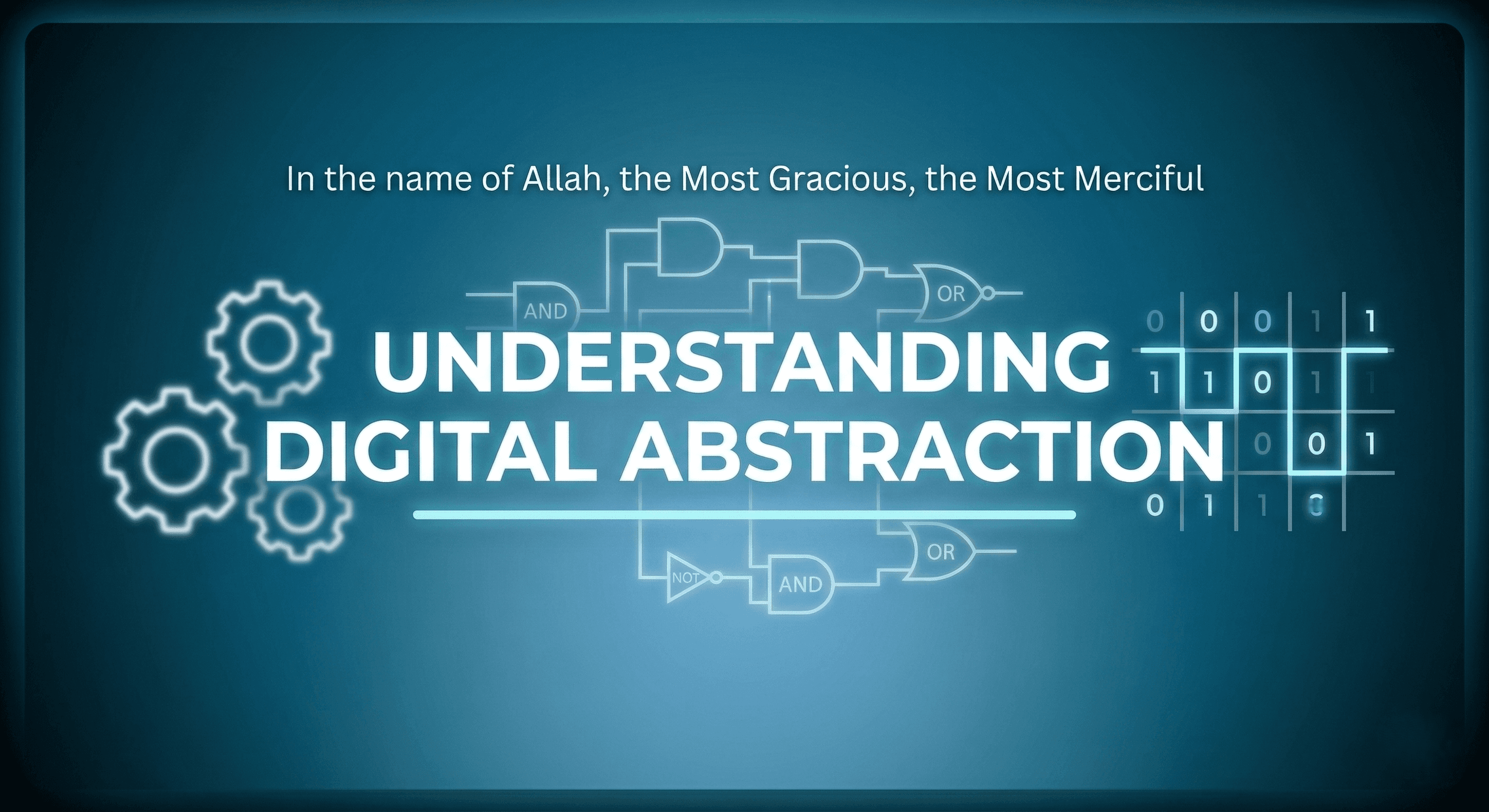
See you in the next lesson! Our first deep dive will be: The Digital Abstraction.